
Creating Nano launches APIS substrate surface cleaning tool
economic daily
September 6, 2023
Author Zhang Jie
September 6, 2023
Author Zhang Jie
Creating Nano Technology, a major domestic manufacturer of normal pressure and low voltage plasma equipment, is committed to the development of atmospheric plasma, anti-fouling, anti-bacterial, anti-fingerprint coating technology and continuous roll-flex transmission based on its superior plasma development capabilities and coating technology. process (roll to roll, R2R), and has made achievements in the development of new processes such as GOG, PEDOT, EMI coating, OLED, and micro LED.
With the advent of the Internet of Things and the future AI generation, the demand for chip heterogeneous integration is gradually emerging, which has also driven the development of advanced packaging and other technical needs. Creating Nano Technology is based on the existing low-pressure reactive ion etching (RIE) equipment. Combined with the patented electrode design, gas flow field uniformization configuration, and fluid cooling system of the substrate stage, it achieves the characteristics of high etching rate, high uniformity and low process temperature, as well as high aspect ratio and anisotropy. Process requirements for etching, etc., suitable for use in related fields such as semiconductors, packaging, and optoelectronics, for processes such as dry etching (Etching) or ashing (Ashing).
Supplemented by the rotating ALD continuous coating technology launched this year, it can not only increase the coating rate and improve the traditional process time, but also improve precise film thickness control and good uniformity, which can target the passivation layer of solar silicon wafers and transistor gates. Oxide layer, semiconductor copper process, and wafer packaging, 2.5D packaging, and 3D packaging applications requiring finer line width and line spacing.

Rotary ALD continuous coating technology.
In order to optimize the coating process, improve output and yield, the newly designed flip mechanism component can effectively shorten the process time and quickly replace the sample system in vacuum. It can also be used for direct sampling analysis to meet experimental needs, simplifying the overall structure and volume.
Because Creating Nano Technology has common technology research and development capabilities with the industry, it has great development capabilities in both touch panels and soft and hard board manufacturing processes. It has been laying out nanomaterials for many years and is constantly looking for them in various industries including panels and semiconductor industries. outlets and development application areas.
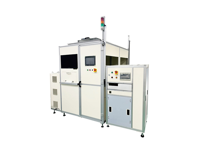
Take the newly developed composite automatic plasma process inspection machine APIS (Advance plasma & inspection system) this year as an example. It mainly uses the high reactivity of plasma to clean the substrate surface and remove residual glue after lamination. It is also targeted at Nai. For meter-level substrate surface planarization applications, this equipment is equipped with a high-precision optical measurement module and is integrated with the Advance Plasma process equipment. Through algorithm calculations, precision processing is performed to achieve substrate planarization. It is suitable for materials that are difficult to machine. For example, SiO2, SiC, etc. can be introduced into AI learning in the future to calculate the substrate topography to greatly increase production capacity.
 Compound automatic plasma process inspection machine APIS.
In addition, for the application of nano-level coating on the substrate surface, the composite automatic plasma process inspection machine APIS can integrate the coating-specific Advance Plasma process module, and the inspection instrument can use a high-precision surface energy measurement module to confirm the surface characteristics of different liquids. It is also equipped with a high-precision automated transfer module to meet substrate surface coating and inspection requirements. Due to the development of coating systems and technologies in various fields, Creating Nano can be said to integrate PVD (sputtering, cathodic arc, filtered arc), PECVD (DLC, colored diamond) and CVD (Ti(C)N, diamond coating) in one.
Taking anti-static dissipation diamond-like carbon (ESD-DLC, DLC) as an example, Creating Nano is well-known in the industry. Through continuous technological advancement, in addition to its original excellent low friction coefficient and wear resistance In addition to the application of wear and corrosion resistance, it is also targeted at the semiconductor field, because as the chip size becomes smaller and smaller, the components used in packaging, sealing and testing and even wafer manufacturing include fixtures (Hot Plate, Change kit, Contact chuck) , tracks, carrier plates, vibration plates, molds, etc., all need to have anti-static functional properties to protect products from damage caused by static electricity during the production process.
 PEALD.
In terms of corporate ESG, Creating Nano uses its technological foundation to develop plasma scrubber, which can effectively destroy and decompose harmful waste gases generated during the coating and etching processes, especially fluorine-containing greenhouse gases, and Combined with the wet cleaning process, the treated waste gas or waste water is discharged, which has obvious benefits in reducing greenhouse gas emissions in the semiconductor process.
Related links: https://money.udn.com/money/story/5635/7419893
【Disclaimer】
The content of this article only represents the author's personal views and has nothing to do with Creating.
The content, textual description and originality have not been confirmed by this website. This website does not make any guarantee or commitment for this article and all or part of its content, authenticity, completeness and timeliness. It is for readers' reference only. Please verify the relevant content by yourself.
Creating Nano Technologies, Inc.
59 Alley 21 Lane 279, Chung Cheng Road, Yung Kang City, Tainan, TAIWAN
TEL:886-6-2323927 FAX:886-6-2013306 URL: http://www.creating-nanotech.com