
The demand for panel-level packaging is booming! Electronics Manufacturing Equipment Exhibition will be held in April, with the first new PLP zone
TechNews
March 24, 2025
Author Lin Yurou
March 24, 2025
Author Lin Yurou
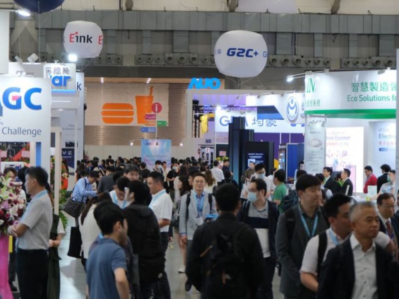
The global semiconductor industry focuses on advanced packaging technology. The "Electronic Production Manufacturing Equipment Exhibition" will debut on April 16. This year, the "PLP Panel Level Packaging Zone" will be added for the first time, focusing on the future key technology "Panel Level Packaging" (PLP for short), and comprehensively displaying the latest equipment, materials and process technologies, and fully presenting a full range of solutions for panel-level packaging from process to equipment, leading the industry to seize the new blue ocean of packaging technology.
During the three days of the exhibition, a series of "PLP Panel-Level Packaging Forums" were held, bringing together AI application giants, semiconductor packaging and testing, panel and IC substrate related manufacturers to participate in the event. More than 50 international heavyweight lecturers including AMD, Applied Materials, Coherent, Schott, Screen, USHIO, Evatec, MacDermid, Foxconn Research Institute, Uwin, Titanium, Mirco and JDT were invited to share the stage. They brought first-hand market views and forward-looking technical analysis on challenges such as global market trends and potential, TGV technology, PLP substrate materials and manufacturing technology, metallization key technology and handling technology, and worked together to accelerate the development and application of PLP technology and lead the industry to upgrade again.
The "PLP Panel-Level Packaging Solution" will be on display from April 16 to 18, bringing together the world's latest advanced packaging technologies, equipment and solutions, to enhance the global competitiveness of Taiwan's semiconductor and electronic equipment industries and to open up new opportunities for a diverse customer base unlike any other.
Related link: https://technews.tw/2025/03/24/e-equipment-2025-panel-level-packaging/
Image source: Taiwan Electronic Manufacturing Equipment Industry Association
【Disclaimer】
The content of this article only represents the author’s personal views and has nothing to do with Creating.
The content, text and originality have not been verified by this website. This website does not make any guarantee or commitment to this article and all or part of its content, authenticity, completeness, or timeliness. It is for readers' reference only. Please verify the relevant content on your own.
Creating Nano Technologies, Inc.
59 Alley 21 Lane 279, Chung Cheng Road, Yung Kang City, Tainan, TAIWAN
TEL:886-6-2323927 FAX:886-6-2013306 URL: http://www.creating-nanotech.com