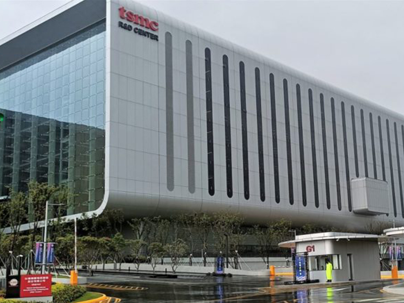
The demand for AI chips is growing rapidly, driving TSMC to actively deploy and develop the High-NA EUV process

TechNewsTechnology News
November 18, 2024
Author Atkinson
November 18, 2024
Author Atkinson
According to media reports, previous market news pointed out that TSMC has received the first set of high numerical aperture (High-NA) extreme ultraviolet (EUV) exposure machine-EXE:5000 from Dutch semiconductor equipment manufacturer ASML in September 2024. This represents TSMC's ever-changing stance on this advanced semiconductor technology. It was cautious at the beginning and then fully developed and adopted in order to maintain its leading position in the highly competitive semiconductor industry and in response to the demand for advanced processes by AI chips. Rapid growth in demand.
According to a report by foreign media techspot, the use of High-NA EUV exposure machines is crucial for TSMC to develop processes below 2 nanometers. Because the High-NA EUV exposure machine increases the numerical aperture from 0.33 to 0.55, it can further achieve higher resolution and more precise imaging operations on the wafer. According to TSMC’s plan, the High-NA EUV exposure machine will be introduced into its A14 node (1.4nm) process, and this process is also expected to enter mass production in 2027.
Currently, these advanced exposure machines will not be immediately operational as rigorous testing, fine-tuning and process optimization are required before they can be integrated into mass production. As for when these exposure machines are fully operational, TSMC is expected to have progressed to its A10 node (1nm) process, which represents several generations of technology beyond its current capabilities. This timeline is also consistent with TSMC's broad path to develop wafer process consistent.
According to reports, at TSMC’s third quarter 2024 press conference, Chief Financial Officer Huang Renzhao outlined the company’s advanced process node development plan. It is stated that TSMC will update the N2 process in 2026, which will cause some preparation costs for updating the N2 process. As TSMC develops each advanced process node, this preparation cost will become larger and larger.
The report emphasized that each set of High-NA EUV exposure machines costs approximately US$384 million. Nonetheless, TSMC’s technological leadership in EUV exposure machines is expected to attract more high-end customers seeking advanced wafer manufacturing capabilities to place orders. That could further widen the gap between TSMC and its rivals, especially South Korea's Samsung Electronics. Because TSMC has laid a solid foundation with its current standard-aperture EUV technology.
Among them, TSMC officially launched the N7+ node process using the EUV process in 2019. At that time, approximately 10 sets of standard EUV exposure machines were in operation. Since then, TSMC has rapidly expanded its EUV production capabilities, which has also caused EUV system sales to grow tenfold between 2019 and 2023. Currently, TSMC accounts for 56% of global EUV exposure machine installations. Continue to utilize it in processes including N5, N3, and next N2 nodes.
TSMC’s approach to EUV is systematic and customer-centric. The company carefully evaluates new technology innovations based on their maturity, cost and potential customer benefits before integrating them into mass production. Therefore, TSMC plans to first introduce High-NA EUV exposure machines for research and development to develop the relevant infrastructure and patterning solutions needed by customers to drive innovation, and then further meet the relevant needs of customers.
Related links: https://technews.tw/2024/11/18/tsmc-actively-deploys-and-develops-high-na-euv-process/
【Disclaimer】
The content of this article represents only the author’s personal views and has nothing to do with Creating.
The content, textual description and originality have not been confirmed by this site. This site does not make any guarantee or commitment for this article and all or part of its content, authenticity, completeness, and timeliness. It is for readers' reference only. Please verify the relevant content by yourself.
Creating Nano Technologies, Inc.
59 Alley 21 Lane 279, Chung Cheng Road, Yung Kang City, Tainan, TAIWAN
TEL:886-6-2323927 FAX:886-6-2013306 URL: http://www.creating-nanotech.com
