
Breaking through decades of technical barriers, scientists create the first graphene semiconductor
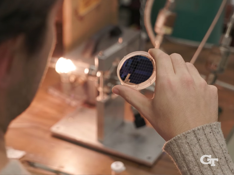
Graphene, which was thought to never be capable of semiconductor work, has made a breakthrough. An international team led by scientists from the Georgia Institute of Technology has successfully created the world's first functional semiconductor made of graphene.
Nearly all components of modern electronics are based on silicon semiconductors, and as development processes become increasingly sophisticated and we approach silicon's energy efficiency limits, it becomes increasingly difficult to use this material to build faster, more powerful computers.
This has prompted physicists to search for new alternative semiconductors.
Now, an international team led by the Georgia Institute of Technology has developed the first extremely strong functional graphene semiconductor with an electron mobility 10 times that of silicon, providing unique properties that silicon does not possess.
Graphene, also known as single-layer graphite, is a honeycomb lattice composed of carbon atoms in sp2 mixed orbitals. It is a strong and widely used flat film material that can withstand extremely large currents without heating up or decomposing.

▲ Graphene structure
Scientists have been developing graphene semiconductors for more than ten years. The challenge lies in the "energy gap" properties of the material - the energy gap from the top of the valence band of a semiconductor or insulator to the bottom of the conduction band, which allows electrons to move around the molecule. Simply put, using engineering techniques to The adjusted energy gap is an important electronic property that controls the conductivity and non-conduction of semiconductors.
However, in its natural form, graphene is neither a semiconductor nor a metal, but a semi-metal. It has no energy gap, so scientists cannot design switches with "correct proportions" of each element to control the graphene semiconductor. Many people also believe that graphene electronics The device never works.
Until now, with the help of a precision induction furnace, a group of researchers has successfully overcome the biggest obstacle in graphene research for decades and created "epitaxial" graphene: growing another layer on a crystal (in this case, silicon carbide) that is chemically bonded to the crystal. The material creates an energy gap and begins to exhibit semiconductor characteristics. Its electron mobility is 10 times higher than that of silicon, or electrons move with extremely low resistance.

▲ Epitaxial graphene has the potential to transform the field of electronics and exploit its unique properties to create new technologies.
Graphene semiconductors are more efficient and do not heat up much. They can be used to make smaller and faster electronic devices and may also be used in quantum computing. The team's sample is currently the only one that has all the necessary properties of nanoelectronics. Two-dimensional semiconductors with electrical properties far superior to any two-dimensional semiconductor currently under development.
The new paper was published in the journal Nature.
- Researchers Create First Functional Semiconductor Made From Graphene
- Graphene semiconductor steps toward ultra-fast computers
Related links: https://technews.tw/2024/01/04/graphene-semiconductor-silicon-energy-gap/
【Disclaimer】
The content of this article only represents the author's personal views and has nothing to do with Kuiding.
The content, textual description and originality have not been confirmed by this website. This website does not make any guarantee or commitment for this article and all or part of its content, authenticity, completeness and timeliness. It is for readers' reference only. Please verify the relevant content by yourself.
馗鼎奈米科技股份有限公司 Creating Nano Technologies,Inc.
59 Alley 21 Lane 279, Chung Cheng Road, Yung Kang City, Tainan, TAIWAN
TEL: 886-6-2323927 FAX:886-6-2013306 URL: http://www.creating-nanotech.com